IMEC Update | Thermal Management Challenges of 3D Integrated Silicon Photonic Circuits
- Latitude Design Systems

- Dec 5, 2023
- 4 min read
Abstract
This paper investigates the thermal effects of three-dimensional (3D) hybrid integration of electronic integrated circuits (EICs) and silicon photonic integrated circuits (PICs) for high-performance optical interconnects. Dense wavelength division multiplexing PIC architectures with integrated ring-based photonic devices are thermally characterized before and after EIC assembly [1]. Thermal measurements and simulations indicate substantial negative impact on photonic device thermal efficiency and crosstalk due to EIC heat spreading. Strategies are explored to mitigate these effects through thermally aware interface designs between EIC and PIC.
Introduction
The exponential growth in internet traffic has necessitated high bandwidth and energy efficient interconnects. Silicon photonics leverages CMOS fabrication to enable large-scale photonic integration, making it suitable for these high-performance links. However, thermal sensitivity of nanophotonic devices presents reliability challenges. Active thermal control through on-chip microheaters enables stable device operation. Furthermore, photonic-electronic convergence is essential, requiring dense 3D integration of PIC and EIC dies using flip-chip bonding. This 3D stacking introduces additional thermal design complexity impacting photonic device performance.
In this work, thermal measurements and multiphysics simulations are conducted on a test vehicle consisting of a PIC with integrated ring modulators flip-chip bonded to a CMOS EIC. Two key metrics - heater efficiency and thermal crosstalk, are extracted before and after EIC integration. The impact of substrate undercuts around photonic devices is also analyzed. These studies enable a quantitative assessment of the thermal penalties introduced through 3D integration as well as provide a pathway to thermal co-optimization of the photonic-electronic interface.

Test Vehicle Description
The test vehicle consists of a 5x5 mm2 silicon PIC fabricated in a CMOS pilot line flip-chip assembled to a smaller 1.5x1 mm2 CMOS EIC using an array of Cu-Sn microbumps at 50 μm pitch embedded in epoxy underfill. The PIC transmit side consists of ring modulators with integrated tungsten microheaters for thermal tuning. Two device variants are characterized - with and without a substrate undercut trench surrounding the silicon waveguide. The EIC provides the electronic driver circuits for the photonic devices. Electrical pads and optical grating couplers provide interfaces to the test setup for electro-optic device measurements.
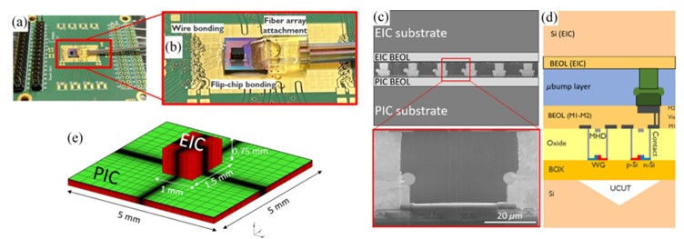
Experiments and Simulation Methodology
Two key device metrics are thermally characterized by tracking the resonance peak shift of ring modulators - heater efficiency and thermal crosstalk between devices. Heater efficiency denotes the resonance wavelength shift per unit power applied to integrated microheater. Lower heater power for a given wavelength shift indicates better efficiency. Thermal crosstalk represents undesired heating of a ring modulator from an activated neighbor’s heater. These metrics are measured at 25°C before and after flip-chip integration of the EIC to quantify the impact of 3D stacking.
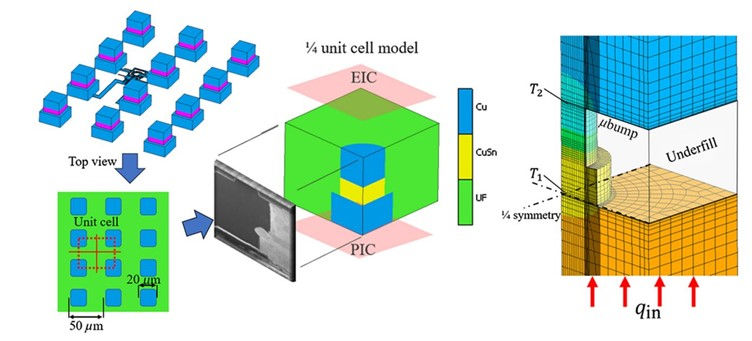
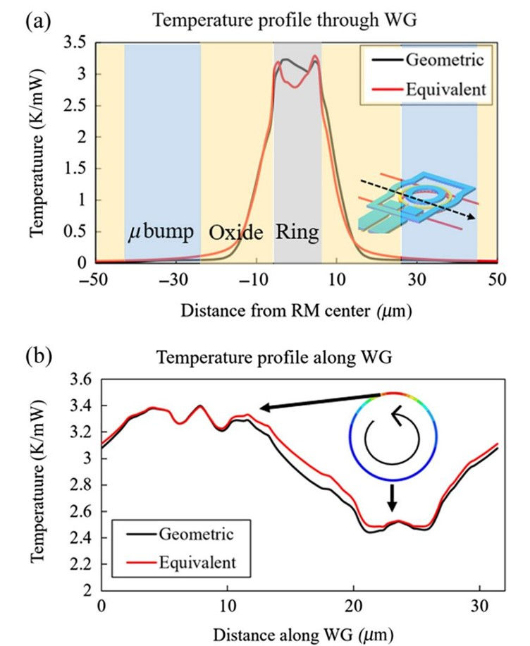
A multiphysics finite element model of the EIC-PIC assembly is constructed with the commercial solver MSC Marc. Joule heating in device microheaters is the simulation input. Convective boundaries, substrate conduction and interface resistances represent packaging effects. Two methods are compared to model the complex microbump interface layer - an actual geometry approach capturing individual bump dimensions and an equivalent property approach with effective conductivities matching the layer cross-section. The waveguide temperature provides the figure-of-merit to assess heater efficiency.
Table 1. Thermal conductivity values for thermal simulations,UF = underfill in μbump layer.
Si | SiO2 | Cu | W | UF | Cu-Sn | BEOL (EIC) | |
Thermal conductivity [W/(m-K)] | 150 | 1 | 400 | 100 | 0.18 | 65 | 1.5 |
Results
1. Heater Efficiency
Experiments indicate a substantial drop in heater efficiency (up to 44%) after EIC integration caused by undesired lateral heat spreading into the EIC acting as a heat sink. This lowers thermal resistance and microheater power efficiency. Both methods for modeling the microbump layer show good agreement with measurements. The EIC presents a parallel path for heat dissipation from PIC devices, offsetting benefits of undercut isolation trenches.
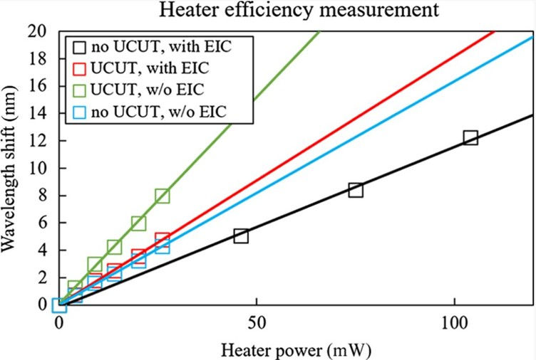
Table 2. Ring modulator heater efficiency from experiments (pm/mW) and simulations (equivalent model) (K/mW). The value between brackets is obtained by the geometric model.
No UCUT | UCUT | |||
No EIC | With EIC | No EIC | With EIC | |
Experiment (pm/mW) | 165 | 131 | 312 | 180 |
Simulation (K/mW) | 3.07 | 2.14 | 5.44 | 2.86 (3.08) |
Simulation (pm/mW) | 192 | 134 | 340 | 179 |
Difference (%) | 16.3 | 2.1 | 8.97 | 0.55 |
2. Thermal Crosstalk
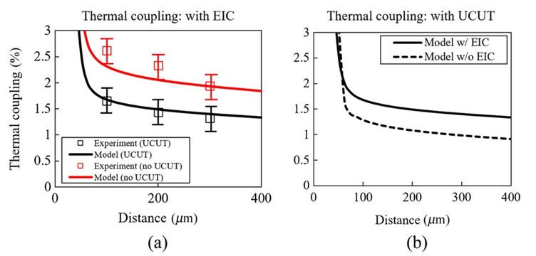
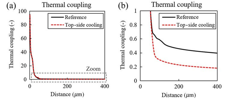
EIC integration increases thermal crosstalk between devices by up to 44% due to additional lateral conduction. However, the model indicates inclusion of top-side cooling solutions can reduce long-range crosstalk by 50%. So while the EIC middleware enhances electrical connectivity, it degrades thermal isolation without careful co-optimization.
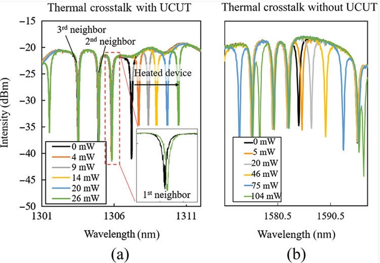
Table 3. Thermal crosstalk experiment and simulation (equivalent model) of EIC-PIC assembly, in percentages.
Distance (μm) | Crosstalk (%) | |||
Experiment | Simulation | |||
No UCUT | UCUT | No UCUT | UCUT | |
100 | 2.62 | 1.65 | 2.32 | 1.68 |
200 | 2.33 | 1.43 | 2.06 | 1.49 |
300 | 1.94 | 1.32 | 1.92 | 1.39 |


Mitigation Strategies and Conclusions
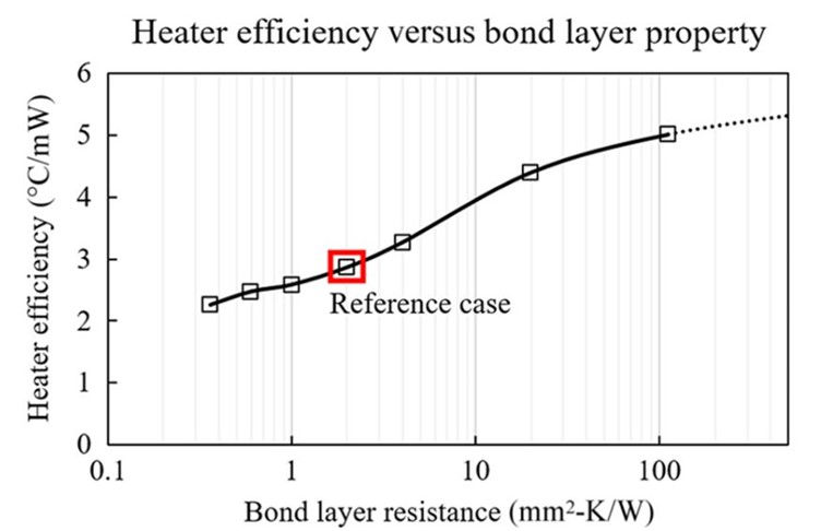
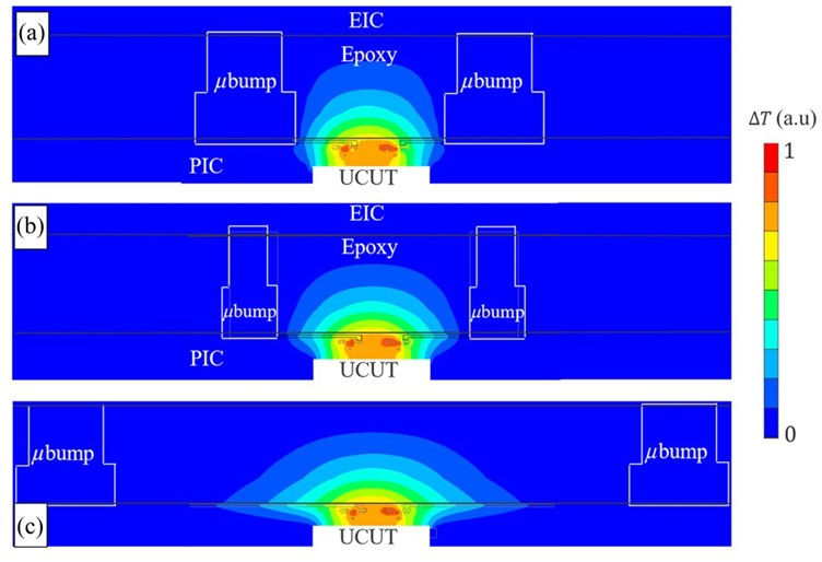
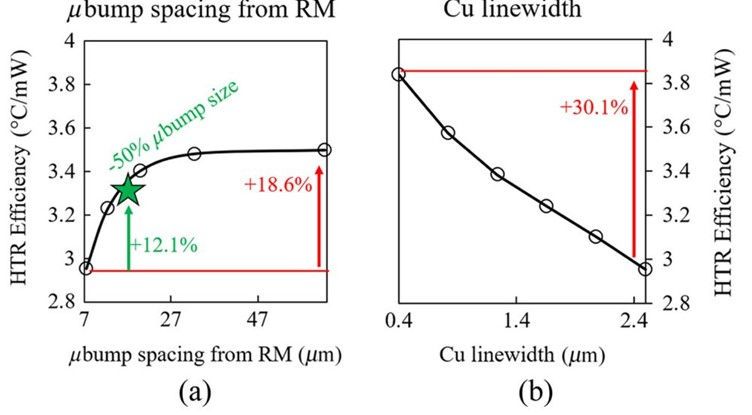
The undesirable thermal effects of the EIC heat spreading can be mitigated through thermally aware co-design of the microbump interface and PIC back-end-of-line metallization. Strategies include:
Maximizing effective thermal resistance of interface underfill
Increasing spacing between microbumps and photonic devices
Reducing metallic linewidth of wiring to microbumps
Simulations indicate combining these techniques can potentially recover >75% of the thermal efficiency loss from EIC integration thereby enabling reliable 3D photonic-electronic modules without significant device performance degradation or power penalties.


Conclusion
This work provides a comprehensive thermal analysis and mitigation roadmap for hybrid integrated silicon photonic interconnects - an emerging technological platform for next-generation high-performance computing and data centers. Thermally co-optimized 3D integration of photonic and electronic dies can unlock performance scaling of these heterogeneous systems.
Reference
[1]D. Coenen, M. Kim, H. Oprins, Y. Ban, D. Velenis, J. Van Campenhout, and I. De Wolf, "Thermal modeling of hybrid three-dimensional integrated, ring-based silicon photonic-electronic transceivers," Journal of Optical Microsystems, vol. 4, no. 1, Jan.-Mar. 2024, Art. no. 011004, doi: 10.1117/1.JOM.4.1.011004.


Comments