Light Monitoring in Standard Silicon Photonics with a Monolithic Transimpedance Amplifier
- Latitude Design Systems

- Nov 26, 2024
- 3 min read
Introduction
Silicon Photonics (SiP) technologies enable the design of large-scale optical systems-on-chip, comprising hundreds of photonic devices capable of performing complex light manipulation. Silicon is an attractive photonic material not only for its excellent optical properties but also because it can be processed using the same manufacturing steps as the microelectronic industry. This allows for the co-integration of electronic and photonic functionalities on the same die, paving the way for next-generation electro-optical systems that exploit the unrivaled bandwidth of optical devices and the versatility of CMOS electronics.
CMOS Transistors in SiP
The integration of complementary metal-oxide-semiconductor (CMOS) devices and digital circuits into a standard SiP process has been demonstrated previously. In this work, the authors further extend this approach by integrating analog electronic circuits into a standard SiP technology, enabling on-chip amplification and processing of electrical signals.
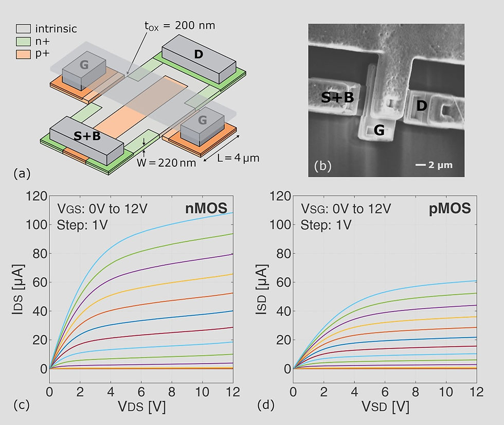
CMOS transistors were integrated into the photonic chip using a zero-change approach, achieved by utilizing only the fabrication steps already available in the standard technological stack of Advanced Micro Foundry (AMF, Singapore). Since metal layers in SiP technologies are relatively far from the silicon, the transistors were designed with lateral silicon gates, exploiting the minimum waveguide-to-waveguide distance of around 200 nm (Figure 1a, 1b).
Both nMOS and pMOS devices were realized, employing the same geometry while inverting the doping species of the diffusion regions. A reasonably low threshold voltage around 1.5 V was achieved thanks to the naturally depleted free carriers in the native silicon layer of a photonic chip. Both devices were electrically characterized, demonstrating successful operation (Figures 1c, 1d), and used to integrate a transimpedance amplifier (TIA) on the photonic chip.

Transimpedance Amplifier for On-Chip Optical Power Monitoring
To implement the TIA, a standard two-stage operational transconductance amplifier (OTA) was designed (Figure 2a). A transdiode current generator biases the input nMOS pair and the active load, while a second Miller-compensated stage provides further amplification and the desired single-pole frequency response. The circuit has a supply voltage of 5 V and a power consumption of 400 μW.
The amplifier was connected in a transimpedance configuration with a feedback resistance of 10 kΩ to read the current signal from integrated germanium photodiodes (PD) and convert it into a voltage directly on the photonic chip. In principle, a battery of TIAs could be used to read any integrated sensor and precisely monitor the optical power in the optical circuit. Moreover, an OTA represents the fundamental building block of many analog electronic circuits and could be used to integrate analog-to-digital and digital-to-analog converters or implement local feedback loops to control and stabilize the behavior of programmable photonic circuits.

Experimental Results
A test structure was designed to characterize the functionality of the TIA, consisting of a straight waveguide that injects light into an integrated photodiode, which is then read by the TIA (Figure 2c). A 90-10 splitter routes 10% of the injected light signal out of the chip for precise comparison with conventional bench-top instruments. TE-polarized grating couplers were used for coupling light in and out of the circuit, each introducing 4 dB of losses.
First, the TIA was electrically characterized by testing its frequency response (Figure 3), both in open-loop and transimpedance configurations. The gain-bandwidth product of the open-loop gain exactly matches the −3 dB bandwidth of the transimpedance gain, confirming the correct design of the circuit and the stability of the amplifier. The resulting bandwidth is about 2 MHz, wide enough to perform effective monitoring of the optical power in most common applications.

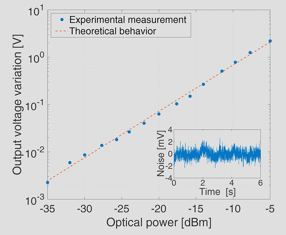
Optical validation was then performed by injecting progressively smaller values of optical power into the chip and measuring the corresponding voltage variation at the output of the TIA (Figure 4). The relation between optical power and output voltage is linear, in accordance with theoretical behavior. The minimum detectable light variation was assessed by measuring the noise at the TIA output without light. A noise RMS value of 660 μV was measured with a readout bandwidth of 1 kHz, corresponding to a minimum detectable light variation of −40 dBm considering the 0.8 A W^-1 responsivity of the PDs.

Conclusion
The successful integration of a transimpedance amplifier in a standard Silicon Photonics technology has been demonstrated. The circuit can successfully read integrated photodiodes up to a frequency of 2 MHz and down to −40 dBm of input optical power, proving the feasibility of on-chip analog processing of electrical signals. This paves the way for the integration of various analog electronic circuits, such as analog-to-digital and digital-to-analog converters, and the implementation of local feedback loops to control and stabilize the behavior of programmable photonic circuits.
Reference
[2] M. Crico, A. Martinez, F. Morichetti, A. Melloni, G. Ferrari, M. Sampietro, and F. Zanetto, "Light Monitoring in Standard Silicon Photonics with a Monolithic Transimpedance Amplifier," Dipartimento di Elettronica, Informazione e Bioingegneria, Politecnico di Milano, 20133 Milano, Italy, 2024.


Comments