
2025 Semiconductor Industry Outlook
- Latitude Design Systems

- Mar 5, 2025
- 3 min read
Global Economic Background and Industry Growth
After experiencing inventory adjustments in 2023, the global semiconductor market is expected to resume growth in 2024. According to the economic outlook report of the organization for Economic Cooperation and Development (OECD), the global GDP growth rate for both 2024 and 2025 is projected to be 3.2%, with varying growth rates across major economies—India leading at 6.2-7.6%, China at 4.2-5.0%, and the U.S. at 1.9-2.8%.
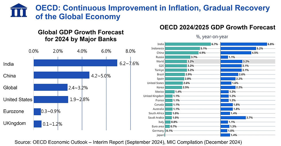
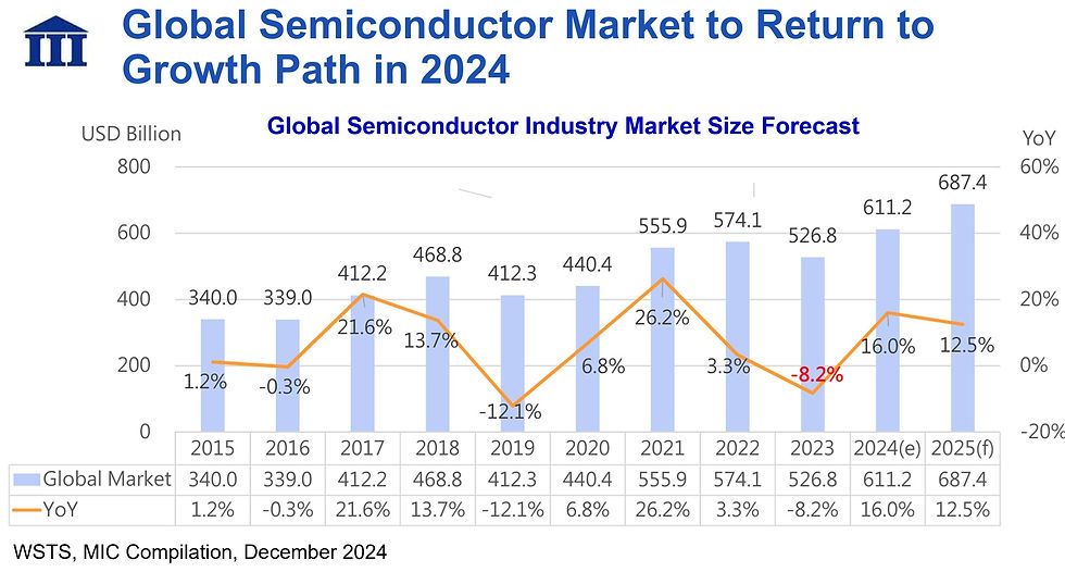
The semiconductor industry’s market size shows a clear recovery trajectory. Historical data indicate that industry experiences cyclical growth, significantly influenced by factors such as the pandemic and supply chain disruptions.
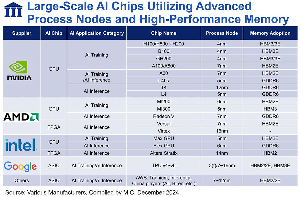
AI-Driven Growth
Artificial intelligence has become a primary driver of growth in the semiconductor industry. The advancement of Large Language Models (LLMs) has created an immense demand for high-performance computing capabilities.
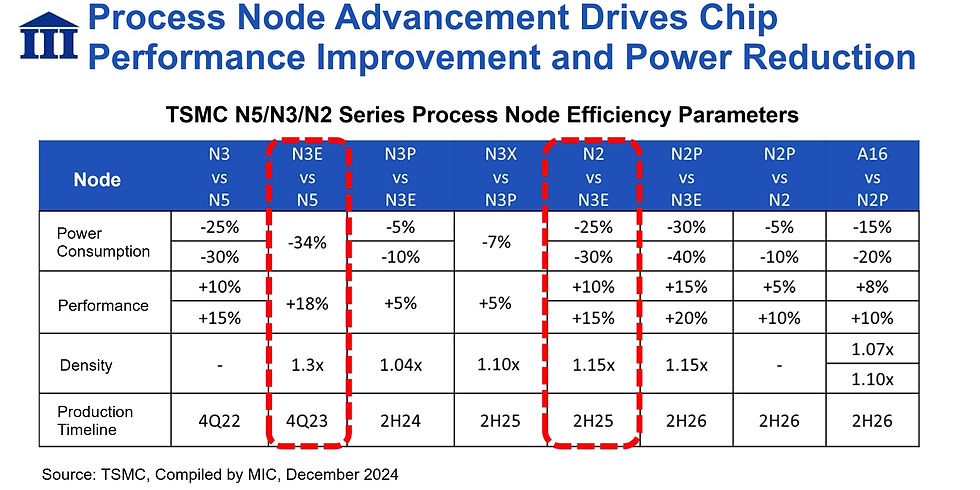
Leading-Edge Process Technologies
TSMC continues to lead in leading-edge process technologies. The company’s technological roadmap demonstrates continuous node advancements, with each generation offering improvements in performance and power efficiency.
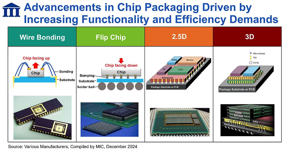
Advanced Packaging Technologies
Significant advancements have been made in semiconductor packaging technologies, driven by the need for improved performance and integration.
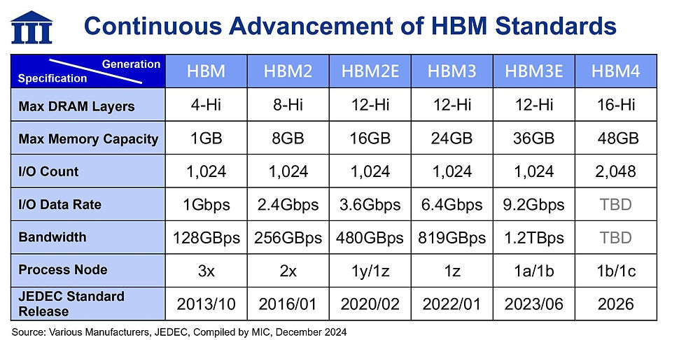
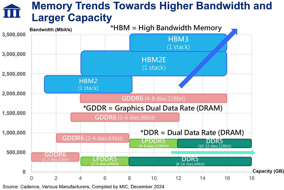
Memory Technology and Integration
High Bandwidth Memory (HBM) technology continues to evolve to meet the demands of AI applications. The progression of HBM specifications indicates continuous improvements in bandwidth and capacity.
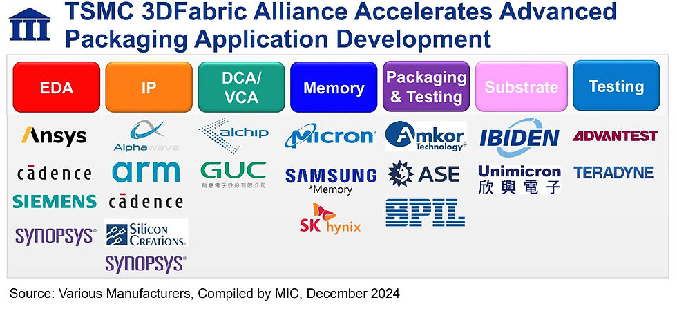
Industry Collaboration and Ecosystem Development
Developing advanced semiconductor technologies requires extensive collaboration within the industry ecosystem. TSMC's 3DFabric Alliance serves as a prime example of such cooperative efforts.
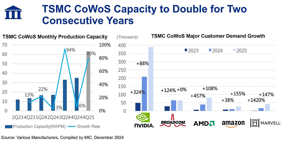
Manufacturing Capacity and Cutting-Edge Technology
TSMC’s CoWoS production capacity continues to expand in response to market demand. By the end of 2024, TSMC’s CoWoS monthly capacity is expected to reach 35,000 wafers, with an annual output projected at 300,000-320,000 wafers. The company further plans to increase its monthly capacity to over 60,000 wafers by the end of 2025.
The continuous advancement in semiconductor process technology has driven improvements in transistor density, power efficiency, and performance. The transition from FinFET to GAAFET has marked significant improvements, with each process generation offering a 5-20% performance boost. Specifically, the N2 process node is expected to deliver a 10-15% performance increase, a 25-30% power reduction, and a 15% increase in transistor density compared to N3E.
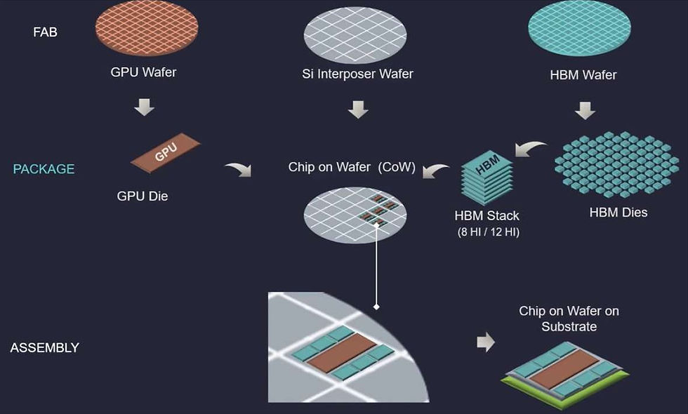
Advancements in Advanced Packaging
The CoWoS technology architecture features complex multi-tiered integration, combining GPU wafers, silicon interposers, and HBM memory in a precise configuration.
Trends in Memory Technology
The development of memory technologies focuses on enhancing both bandwidth and capacity. Different memory solutions are optimized for specific application scenarios, balancing trade-offs between bandwidth and storage capacity.
Future Outlook
Driven by AI applications, the semiconductor industry is expected to sustain its growth trajectory. However, several challenges remain:
Massive investment requirements for advanced process technologies
Increasing demand for supply chain resilience
Physical limitations in process node scaling
Geopolitical uncertainties affecting industry
The establishment of strong technology partnerships and innovative ecosystems will play a crucial role in the industry's future development. Semiconductor companies must maintain a balanced approach in R&D investments, strategic collaborations, and geopolitical considerations to ensure sustainable technological progress and industry growth.
References
[1] K. Cheng, "2025 Semiconductor Industry Outlook and Key Issues," [Technical Presentation], Institute for Information Industry, Taipei, Taiwan, Dec. 4, 2024.


Comments