
IEDM2024|CMOS-Integrated Subtractive Microfluidics as a Novel Lab-on-Chip Platform
- Latitude Design Systems

- Apr 14, 2025
- 3 min read
Introduction
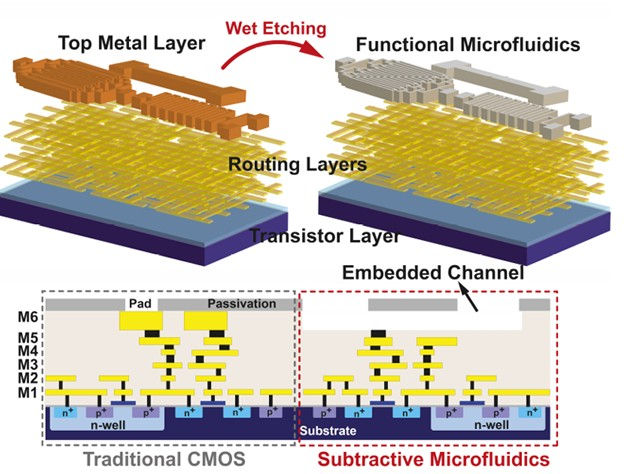
Subtractive microfluidics fabricates fluidic channels by selectively removing metal layers from CMOS chips, tightly integrating microfluidic technology with CMOS processes. This achieves analytical functionalities in a compact, chip-scale laboratory platform [1].
Technology Overview
Subtractive microfluidics utilizes the backend metal interconnect layers in CMOS chips as sacrificial materials. Through controlled wet etching, these metal layers are removed to form precisely defined fluidic channels. Compared to traditional methods, this technique offers multiple advantages, including perfect alignment between electronic components and fluidic channels, high integration, and scalability down to sub-micron dimensions.
Fabrication Process
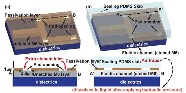
The process begins with standard CMOS chips containing predefined metal patterns, which serve as the blueprint for fluidic channels. To enhance etching efficiency, small pad openings are strategically placed along the channels. These openings provide additional access points for etchants, significantly improving the removal efficiency of metal layers. After etching, the openings are sealed using PDMS (polydimethylsiloxane) microfluidic structures.
System Assembly and Integration
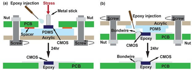
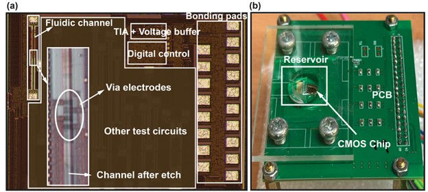
The system assembly process involves several key steps to ensure the proper functionality and protection of electronic components. First, the CMOS chip is embedded into a PCB using biocompatible epoxy resin, followed by wire bonding and encapsulation. During assembly, the PDMS layer protects the chip surface and additional PDMS structures are added for fluid transport.
Integrated Sensing Functions
The platform directly integrates multiple sensing modalities with microfluidic channels:
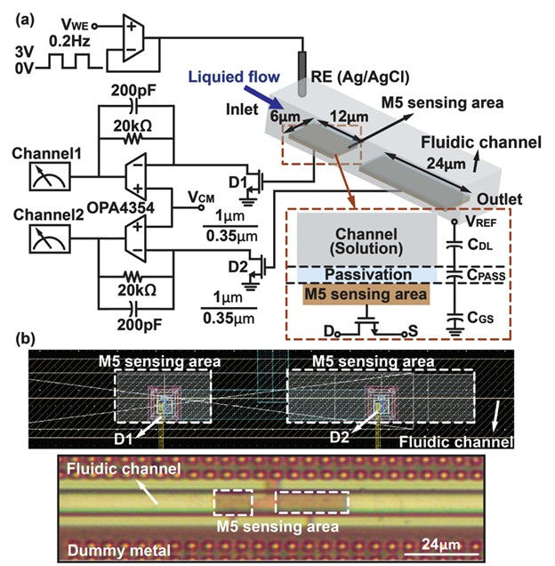
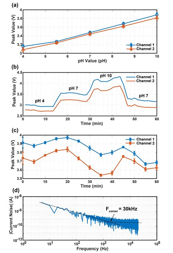
Ion-sensitive field-effect transistors (ISFETs) implemented using thick-oxide NMOS transistors enable pH sensing. The sensing region is defined by metal layer M5 and includes two different sizes (6µm × 12µm and 6µm × 24µm), exhibiting different sensitivities.
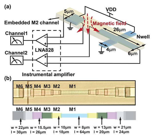
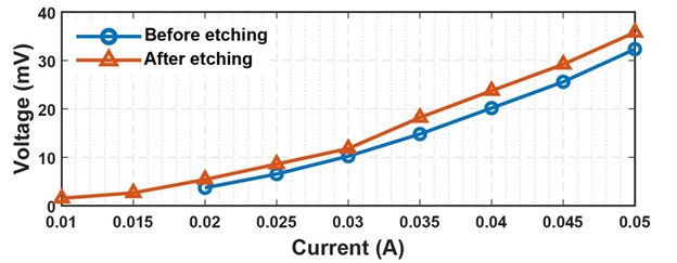
Hall sensors based on N-well resistors enable magnetic field detection. These sensors remain functional after the etching process. While some offset voltage is introduced, it can be compensated through circuit techniques.
Impedance Sensing System
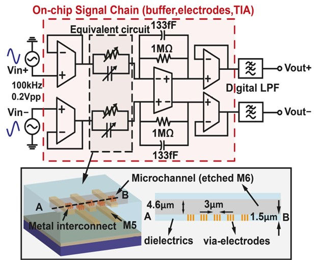
This platform includes a fully differential impedance sensing system with integrated readout circuits. The vias between metal layers M5 and M6 serve as fluid-interface electrodes, exposed during the channel formation process.

Performance and Applications
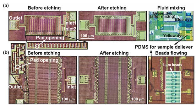
The subtractive microfluidics platform successfully realizes various microfluidic structures, including micromixers and 1:64 splitters. The integrated sensors exhibit reliable performance: ISFETs demonstrate pH sensitivity, and Hall sensors maintain stable magnetic field detection capabilities. The impedance sensing system effectively measures different ionic concentrations and can be applied in cell detection and analysis.
This innovative microfluidic integration method within CMOS technology is suitable for highly integrated, high-throughput lab-on-chip applications. The platform combines complex electronic functionalities with precise fluid handling capabilities, offering significant advantages for point-of-care diagnostics and bioanalytical applications.
Reference
[1] W.-Y. Weng, A. Di, X. Zhang, Y.-C. Tsai, Y.-T. Hsiao, and J.-C. Chien, "Subtractive Microfluidics in CMOS," in 2024 IEEE International Electron Devices Meeting (IEDM), San Francisco, CA, USA, 2024.


Comments