
IEDM2024|Scalable Classical and Quantum Photonics Technologies
- Latitude Design Systems

- May 16, 2025
- 3 min read
Introduction: Evolution of Photonic Systems
Photonics technology has demonstrated significant advantages in computing and communication platforms, offering faster operation, smaller size, and higher energy efficiency compared to traditional electronic systems. However, the integration scale of current photonic systems still lags electronics. This is primarily due to conventional design methods resulting in bulky circuits, low efficiency, and high sensitivity to manufacturing and environmental changes. Additionally, many emerging applications, especially quantum systems, demand novel materials beyond silicon and innovative heterogeneous integration processes [1].

Innovative Approach: Photonic Inverse Design
Revolutionizing photonic design methods has dramatically enhanced device performance. Inverse design methods utilize computer software to systematically explore all possible geometric structures, employing optimization strategies that consider manufacturing constraints. This process integrates GPU-based high-speed electromagnetic solvers with gradient descent optimization algorithms, yielding new photonic devices and systems with performance far exceeding traditional designs.
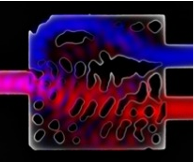
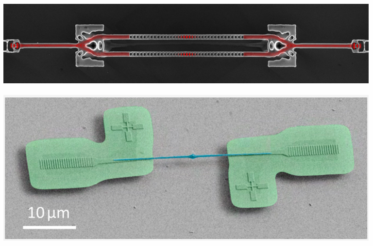
Inverse design methods excel particularly in creating wavelength demultiplexers, essential components of optical communication systems. These devices significantly reduce occupied space while maintaining efficiency comparable to conventional designs and exhibit stable performance under temperature variations.

Breakthroughs in Classical Photonics Technology
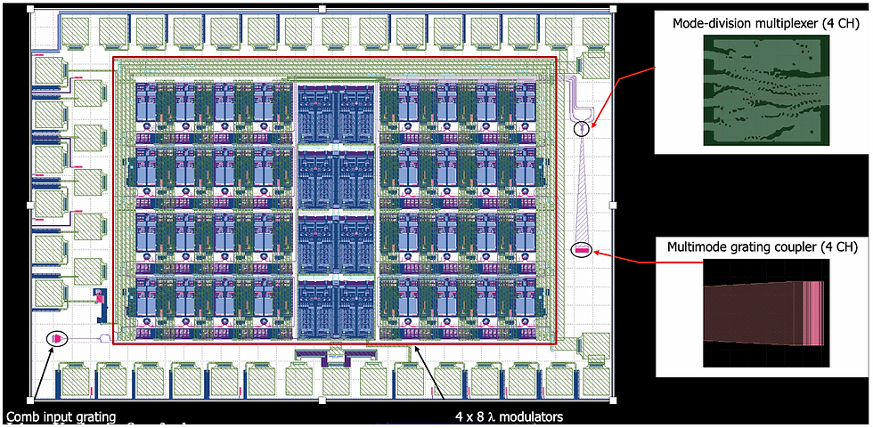
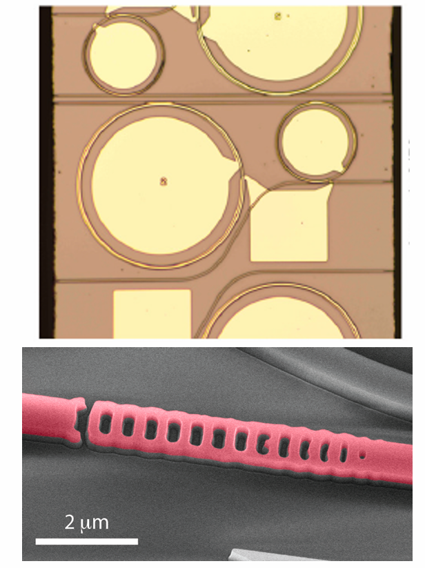
The development of inverse-designed components has led to breakthroughs in classical photonics systems. A significant achievement includes the development of error-free TB/s communication systems for intra-chip and inter-chip optical interconnects.
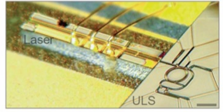
Another key advance in laser technology is the miniaturization of the titanium sapphire laser, a cornerstone of optical laboratories. This accomplishment significantly reduces system size while preserving performance comparable to commercial desktop systems.

Developments in Quantum Photonics Technology
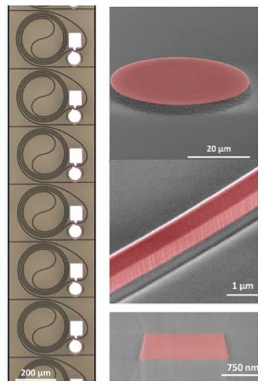
Significant progress has been made in quantum photonics, especially in the development of diamond and silicon carbide color centers. Recent achievements include high-fidelity microwave control of electron spin states at 1.7K and precise single-shot optical readout capability.
Silicon carbide has emerged as an ideal platform for quantum technologies. Its CMOS compatibility and strong optical nonlinearity make it particularly suitable for generating quantum states such as squeezed light, applicable in quantum metrology and continuous-variable quantum computing.
Recent research has demonstrated coherent controlled interactions among multiple quantum emitters within a single silicon carbide resonator, establishing these systems as viable for quantum simulations and potentially quantum computing applications. The integration of quantum emitters with photonic circuits is a crucial step toward scalable quantum technologies, supporting applications such as quantum networks, quantum simulations, and quantum computing.
The convergence of classical and quantum photonic technologies, driven by advanced design methodologies and manufacturing techniques, is propelling the development of next generation integrated photonic systems. These advancements will stimulate innovation in classical communication systems and quantum technologies, significantly enhancing information processing and communication capabilities.
Reference
[1] J. Vuckovic et al., "Scalable classical and quantum photonics," in 2024 IEEE International Electron Devices Meeting (IEDM), San Francisco, CA, USA, 2024.


Comments