The Next Wave of Computing with Optical I/O
- Latitude Design Systems

- May 2, 2024
- 4 min read
Introduction
As artificial intelligence and machine learning models continue to grow exponentially in size and complexity, traditional computing architectures are struggling to keep up with the demands for increased compute power, memory capacity, and bandwidth. To enable the next wave of computing, a paradigm shift is required in how we design and interconnect the various components within these systems. This is where optical input/output (I/O) technology comes into play, offering a solution that can revolutionize the way we build and scale high-performance computing (HPC) and AI/ML infrastructures.

The Growing Demand for Compute and Memory
The number of parameters in AI and ML algorithms is increasing at an astonishing rate, with some estimates suggesting a 35-fold increase in just two years and a 100-fold increase in three years. This rapid growth means that we need to scale the amount of compute and memory resources available, tightly integrating them to solve these complex problems efficiently. A single accelerator, such as a GPU, can typically handle up to a billion or 10 billion parameters, but to support trillions of parameters, we need an infrastructure that can handle hundreds of terabytes of memory and exaflops of compute power.

The Need for Efficient Interconnects
Traditional computing architectures rely on electrical interconnects, but as the distance between components increases, these interconnects face significant challenges in terms of bandwidth density, energy efficiency, and latency. The bisection bandwidth – the bandwidth available for communication between two halves of a system – is often limited by the cost, power, and efficiency constraints of electrical interconnects.
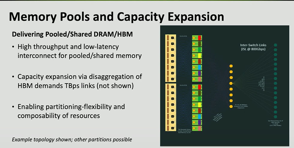
To address these limitations, we need an efficient way to interconnect distributed elements that carry compute capability and large amounts of fast memory. This is where optical I/O comes into play, offering a solution that can break the distance barrier and enable high-radix, high-throughput links between components.

The Promise of Optical I/O
Optical I/O chiplets represent a promising approach to enabling the next wave of computing. These chiplets integrate directly into the package, surrounding the system-on-chip (SoC) die and offering multiple fiber ports. Each chiplet can provide a certain number of ports, with each port carrying data over multiple wavelengths simultaneously.
The interface between the SoC die and the optical I/O chiplet can be highly efficient, with ultra-low power consumption per bit transmitted. This approach allows for direct optical connectivity out of the package, enabling high-bandwidth, energy-efficient communication over longer distances.
One key advantage of optical I/O chiplets is that they leverage an external multi-wavelength light source, solving thermal challenges associated with integrating lasers within the package itself. This external light source can produce multiple wavelengths, allowing for parallel data transmission over multiple carriers per port and per chiplet.


The Value Proposition of Optical I/O
Electrical interconnects excel at short distances, such as within a package or on a board, but their performance degrades rapidly as the distance increases, particularly at very high throughput rates like 100 Gbps or 200 Gbps per lane. Optical interconnects, on the other hand, can maintain high bandwidth density and energy efficiency over longer distances, making them ideal for off-board and rack-scale interconnects.
By integrating optical I/O chiplets into the package, we can effectively extend the benefits of in-package electrical interfaces, such as ultra-low power consumption and high bandwidth density, to optical interconnects. This enables us to transcend the limitations of the package or substrate and create a rack-scale interconnect that behaves almost as if all components were on the same package, with low latencies, high throughput, and efficient power consumption.

Scaling Optical I/O Technology
The multi-wavelength micro-ring-based chiplet technology used for optical I/O offers significant scalability potential. Current demonstrations showcase eight ports per chiplet, with eight wavelengths per port, and 32 Gbps per wavelength using non-return-to-zero (NRZ) modulation. This translates to a bidirectional throughput of 4 Tbps per chiplet, with a clear path towards doubling or further scaling this performance.
Advancements in the technology include increasing the number of ports per chiplet, the number of wavelengths per port, and the data rate per wavelength. Additionally, multiple chiplets can be integrated into a single package, limited only by the available shoreline (the perimeter available for I/O connections).


Ecosystem Development and Standardization
While optical I/O technology holds immense promise, its widespread adoption requires the development of a robust ecosystem and standardization efforts. Key areas for standardization include form factors, fiber management solutions, connectors, packaging infrastructure, and testing methodologies.
Ongoing demonstrations and collaborations within the industry aim to showcase the capabilities of optical I/O and drive the development of this ecosystem. For instance, recent demonstrations have integrated optical I/O chiplets into FPGA packages, enabling multi-terabit connectivity between accelerators on a card form factor.
Conclusion
The next wave of computing, driven by the insatiable demand for AI and ML capabilities, requires a paradigm shift in how we design and interconnect compute and memory resources. Optical I/O technology, particularly in the form of integrated chiplets, offers a promising solution to address the limitations of traditional electrical interconnects.
By enabling high-bandwidth, energy-efficient, and low-latency communication over longer distances, optical I/O chiplets pave the way for rack-scale interconnects that can span multiple chassis or racks, effectively redefining the concept of a "socket" or "super-chip." With significant scalability potential and ongoing ecosystem development efforts, optical I/O technology is poised to play a pivotal role in enabling the next wave of computing, unlocking new frontiers in AI, ML, and HPC capabilities.
Reference


Comments